FPGA architecture
The BrightEyes-TTM implementation was conceived and designed having in mind the fluorescence applications thus providing a good compromise between cost, photon-timing precision and resolution, temporal range, electronics dead-time, maximum photon-flux. The low FPGA resource in the current implementation ensures the highly scalability of the architecture, potentially enabling more channels and, in general, new applications. We chose an FPGA approach to grant both quick prototyping and versatility, and to give the miscroscopy community the posibility of further modifing the TTM depending on future and always-evolving needs.
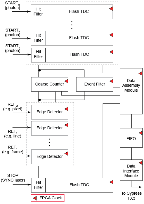
Fig.2 - BrightEyes TTM architecture
VHDL source code TTM architecture components:
Hit filter - The hit-filter component is engineered and deployed to shape the incoming photons and sync signal lengths based on the sampling FPGA clock period and, at the same time, for generating a toggle signal event (the photon or sync enable signal) for each detected photon or laser pulse event.
Flash TDC - The core constituent of the flash TDC module is a tapped delay line (TDL). The TDL is made up by a series of small delay elements (CARRY4 elements for the Kintex-7 FPGA used - for more info check page 43 of 7 Series FPGAs Configurable Logic Block User Guide joined in a chain architecture and is used to delay an input (photon/START) signal with respect to a reference-sampling FPGA digital clock. Whitin the Flash TDC module also a thermometer-to-binary encoder (T2B) is embedded: a dedicated FPGA circuit is needed to interpret and decode the TDL output data. The T2B converts the TDL readout into a binary format allowing for a more effective data registration in terms of memory resources utilisation.
FIFO memory - First-In First-Out (FIFO) internal FPGA memory used to store the registered photons and laser sync events before sending their info out to a host processing unit.
Data interface module - Module component that allows the data to be transfered from the FPGA to the EZ-USB® FX3™ SuperSpeed Explorer Kit.
In the v2 version there is a datapreparation and datapreparation_zerosuppression. The first packs the data according to the v2 protocol and the second module avoid to transmit the channel data which are not hit.
In the v1 version the data are packet directly in the Flash TDC.
Note
Input map
The version v2.0 have two top module. In the Vivado project one must be disabled and the other one must be enabled and selected as Top module:
top_diff.vhd (which needs top_diff.xdc enabled - for differential inputs - designed the SPAD7x7-to-FMC adapter board )
top_single_ended.vhd (which needs top_single_ended.xdc enabled - for single-ended inputs - designed for SMA/SMB-to-FMC adapter board )
The BrightEyes-TTM architecture (Fig.2) combines N+1 (N = 25 photon channels in this implementation) tapped delay lines (TDLs) and a coarse counter running at 240 MHz to obtain N fine TDCs with tens of picoseconds precision (for the start-stop time of each photon channel), and M coarse TDCs with a nanosecond precision (M = 3 reference channels in this implementation).